SOI (Silicon-on-Insulator), namely silicon on an insulating substrate, can also be defined as a silicon wafer structure where an insulating layer is inserted between the substrate and a thin top silicon layer. Currently, there are four mainstream fabrication technologies: SIMOX (Separation by Implanted Oxygen), BESOI (Bonding and Etch-Back SOI), Smart-Cut, and Sim-bond (Oxygen Implantation Bonding) technology.
Classified by fabrication technology, SOI wafers are divided into four types: SIMOX, BESOI, Smart-Cut, and Sim-bond SOI wafers.
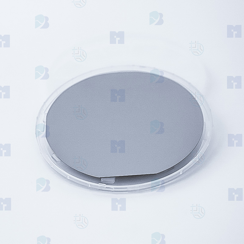
Diameter: 2 ~ 8 inches;
Device layer thickness: 100 nm ~ several tens of μm;
Resistivity: various grades available;
Buried oxide layer thickness: customizable;
Geometric parameters: TTV (Total Thickness Variation), WARP, BOW and other key indicators.
SOI wafers are mainly applied in the high-end chip fields demanding low power consumption, high performance and high reliability, such as RF front-end modules, automotive electronics, aerospace, and advanced microprocessors, etc.
SOI wafers feature outstanding properties including low parasitic capacitance, high integration density, fast operating speed, simplified fabrication process and reduced short-channel effect. All SOI wafers supplied by our company are manufactured by top-tier semiconductor enterprises, with uniform and dense buried oxide (BOX) layers and guaranteed product quality. We maintain a sufficient inventory of SOI wafers, supporting minimum order quantity (MOQ) of 1 piece, and also provide custom processing services as required.