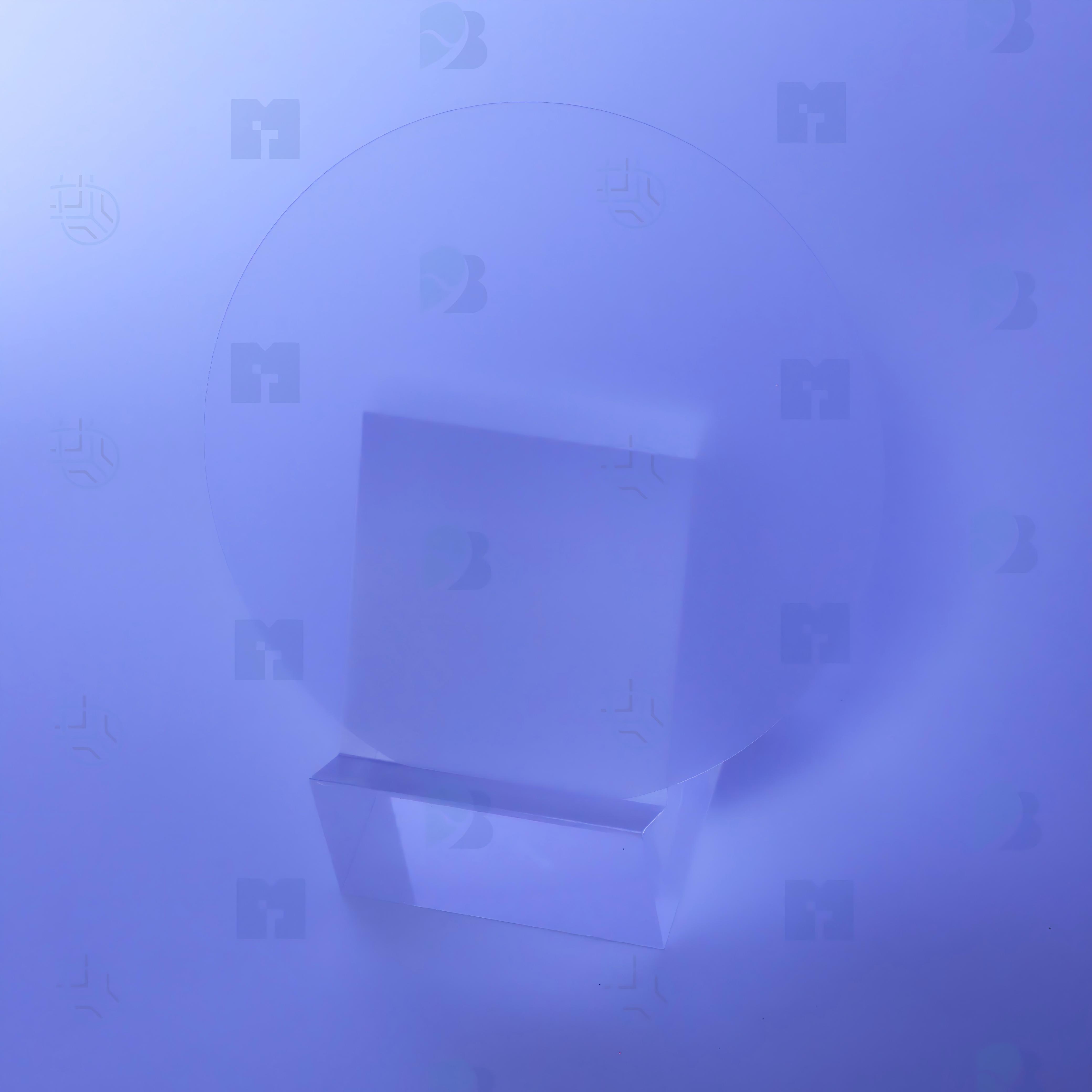
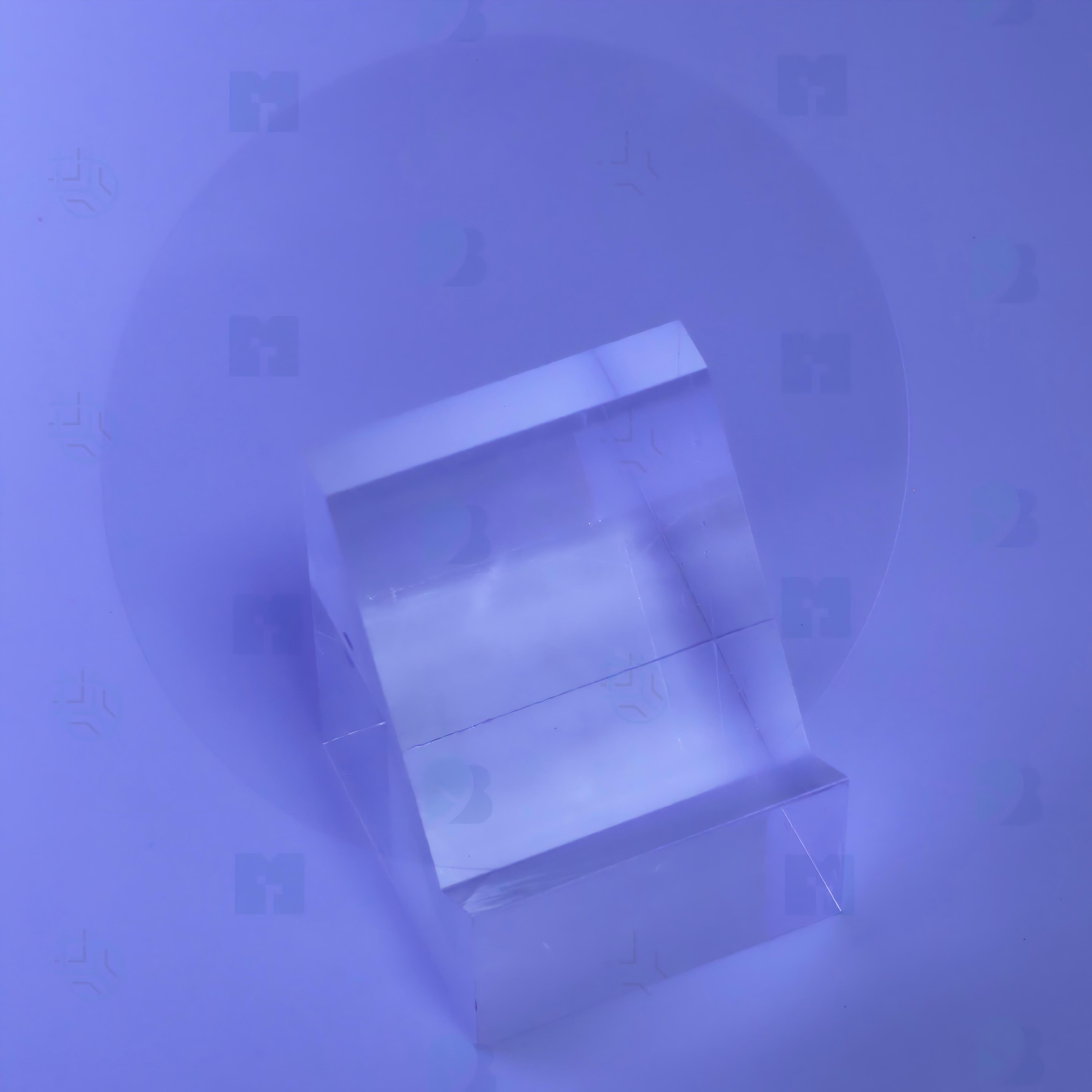
Sapphire wafers, also known as alumina wafers, have a chemical composition of aluminium oxide (Al₂O₃) and feature a hexagonal crystal lattice structure.
Classified by crystal orientation cuts, they are divided into A-Plane, C-Plane and R-Plane sapphire wafers.
Diameter: 2 ~ 8 inches;
Surface treatment: single-side polished / double-side polished;
Crystal orientation: C<0001>, M<10-10>, A<11-20>, R<1-102> and other orientations;
Thickness: 150μm ~ 1mm (customization available for thicker dimensions).
Sapphire wafers are widely used for the epitaxial growth of III-V and II-VI compound semiconductors (e.g., GaN, AlN) as well as various semiconductor thin films.
They are also applied in the fabrication of semiconductor optoelectronic devices (e.g., LEDs, lasers), RF devices demanding high stability, high temperature and corrosion resistance, and are further utilized in LED lighting, consumer electronics, optical communications, aerospace and other fields.
Our sapphire wafers are fabricated from high-purity monocrystalline Al₂O₃ optical grade 1 materials, featuring low lattice mismatch rate, stable physical and chemical properties, ultra-low surface roughness, excellent flatness and high cleanliness. They exhibit outstanding light transmittance ranging from the near-ultraviolet (190nm) to the mid-infrared spectrum.