Quartz wafers are classified into fused silica wafers and single crystal quartz wafers. Fused silica wafers are typically fabricated by cutting and grinding fused silica glass, with a silicon dioxide (SiO₂) content of over 99.99%. Single crystal quartz is composed of high-purity SiO₂; its crystal structure varies at different temperatures under atmospheric pressure.
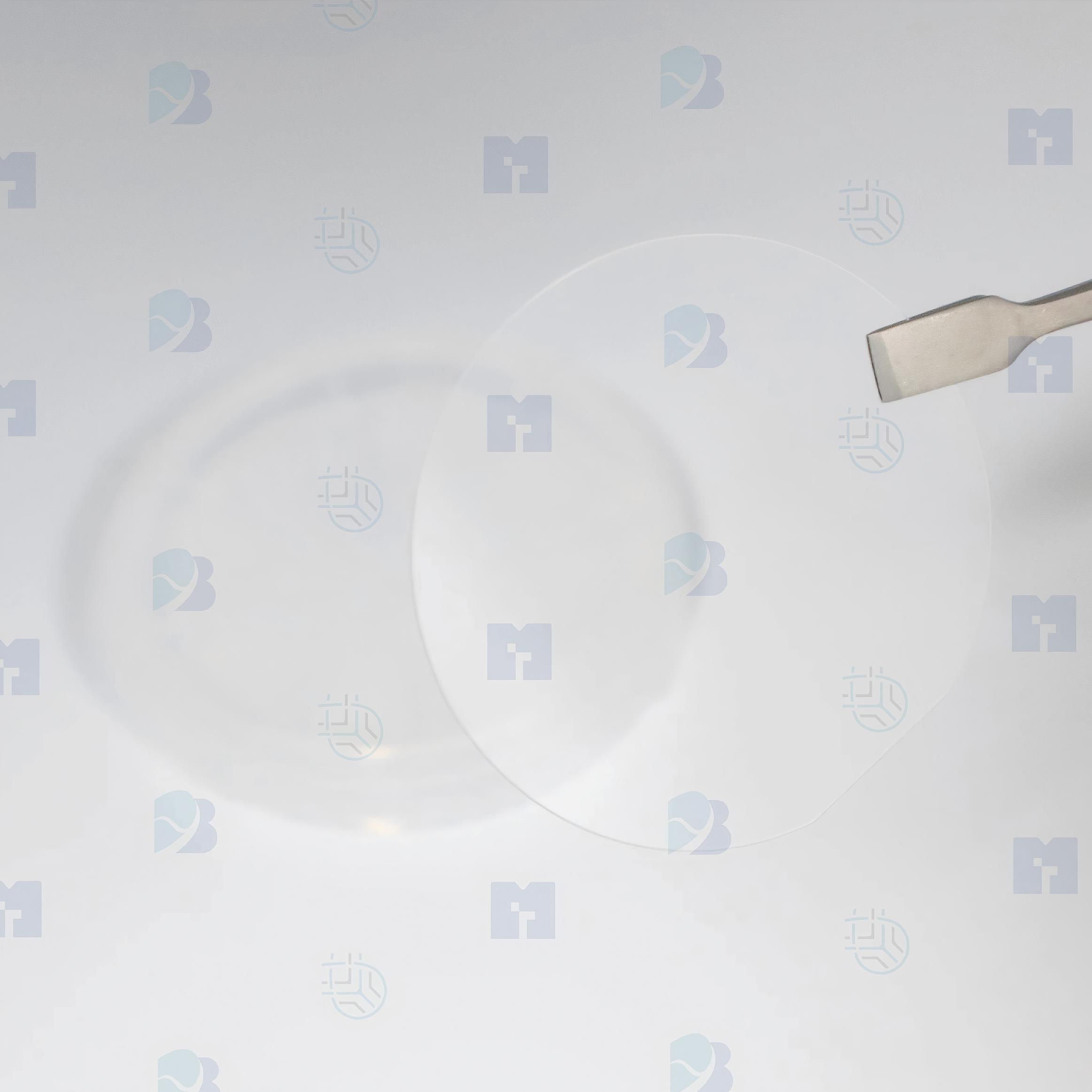
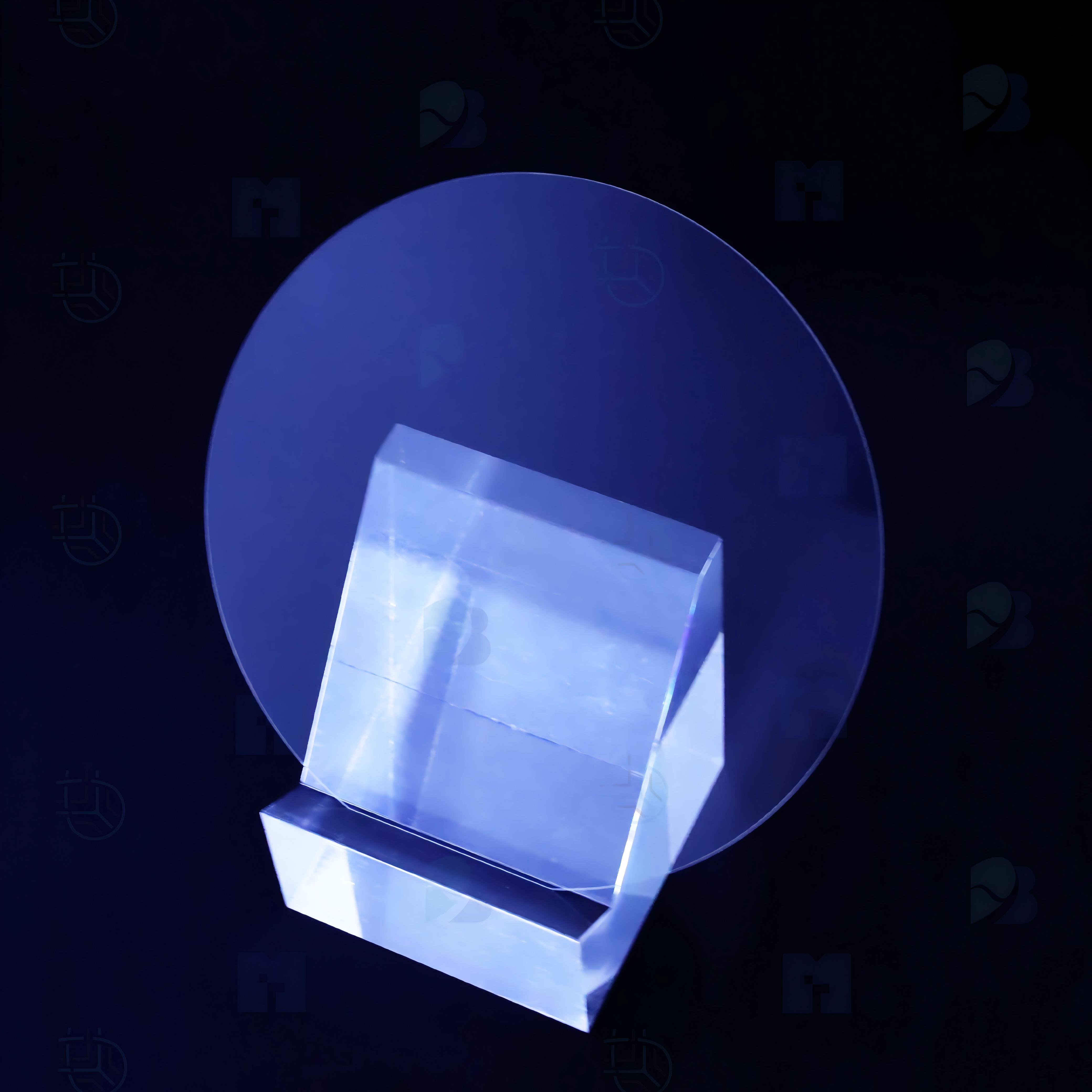
Fused silica glass wafers and single crystal quartz wafers.
Fused silica glass wafers are graded as JGS1, JGS2, JGS3, etc;
Single crystal quartz wafers offer a variety of crystal cuts: X-Cut, Y-Cut, Z-Cut, ST-Cut, AT-Cut, etc;
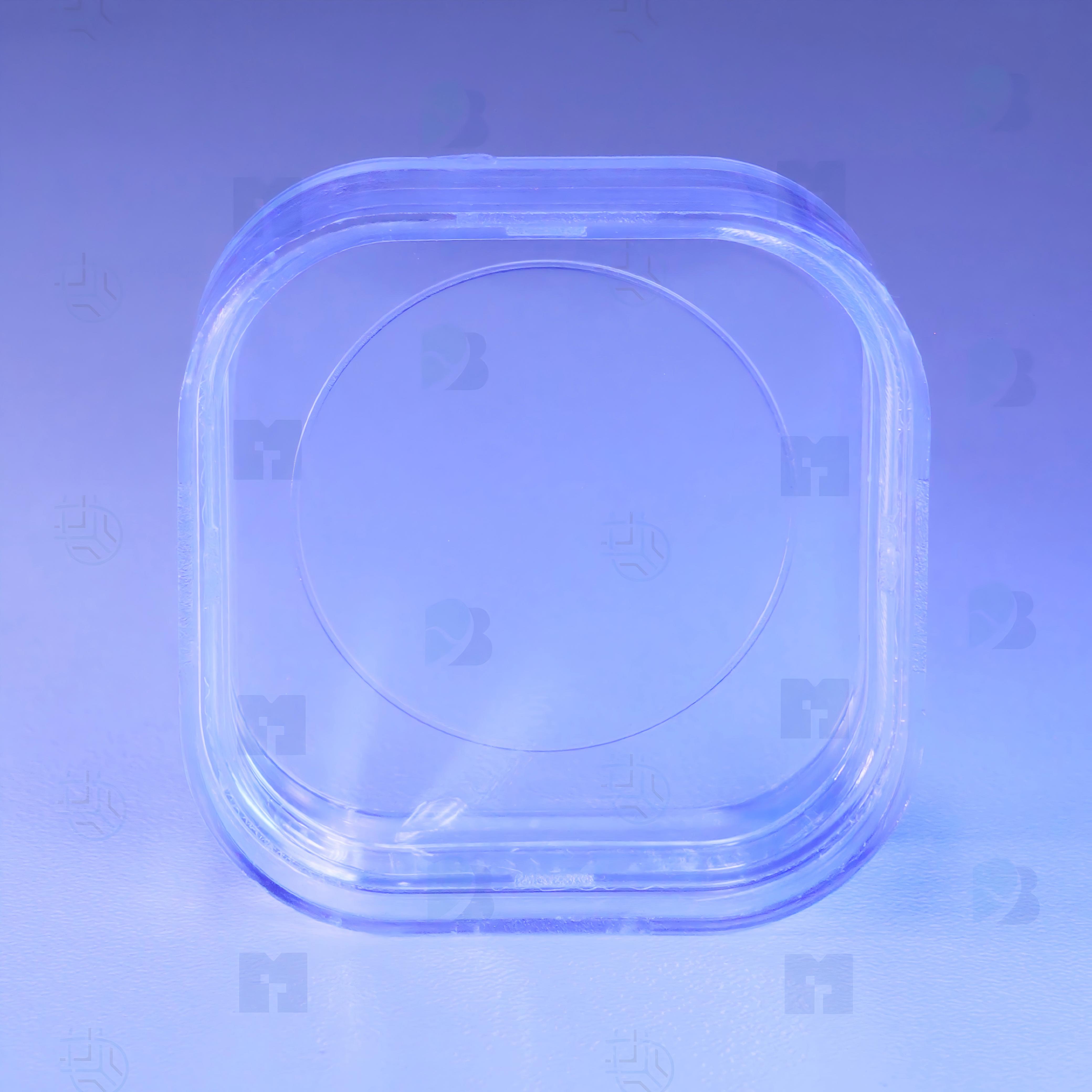
Surface treatment: double-side polishedDiameter: 2 ~ 12 inches;
Thickness: 200μm ~ 1mm (customization available for thicker dimensions).
Fused silica wafers are mainly used in manufacturing semiconductor process devices (e.g., photomasks, wafer carriers) and optoelectronic devices that require high purity, high stability and excellent optical performance. They are also widely applied in integrated circuit (IC) manufacturing, optical communications, precision optics, aerospace and other fields.
Single crystal quartz wafers are primarily used for fabricating frequency control and selection devices (e.g., resonators, filters) that utilize its piezoelectric effect, and are extensively employed in high-frequency precision electronic fields such as communication equipment, consumer electronics, and navigation systems.
Fused silica wafers feature high temperature resistance, excellent electrical insulation, superior light transmittance and corrosion resistance.
Single crystal quartz wafers exhibit a prominent piezoelectric effect, enabling a wide range of application scenarios.
Both fused silica wafers and single crystal quartz wafers boast high cleanliness, flat and uniform surfaces, with guaranteed product quality.